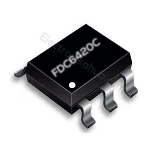
These devices have been designed to offer exceptional power dissipation in a very small footprint for applications where the bigger more expensive SO−8 and TSSOP−8 packages are impractical.
Features
- Q1 3.0 A, 20 V
♦ RDS(on) = 70 m @ VGS = 4.5 V
♦ RDS(on) = 95 m @ VGS = 2.5 V - Q2 −2.2 A, −20 V
♦ RDS(on) = 125 m @ VGS = −4.5 V
♦ RDS(on) = 190 m @ VGS = −2.5 V - Low Gate Charge
- High Performance Trench Technology for Extremely Low RDS(on)
- SUPERSOT−6 Package: Small Footprint (72% Smaller than SO−8); Low Profile (1 mm Thick)
- This is a Pb−Free Device
Applications
- DC−DC Converter
- Load Switch
- LCD Display Inverter




Reviews
There are no reviews yet.